Notes on Computers
The inner workings of Computer Architecture.
The inner workings of Computer Architecture, aggregated from several classes, my life and studies, an ongoing thing….
I am at a Graduate level now in Computer Science with more career experience, I am unsure on a Doctoral Dissertation but may pursue one dependent on other factors…
For now, this is work spanning my personal inferences and some college courses, will continue to proofread and add anything interesting...
Hello, the image you see here is also named Colossus (from the Marvel universe appearing in 1975) that shares an unrelated namesake of one of America’s first computers that I always found cool. Moving on to other, real popular images below of the room-sized computers built since the 1940s...

The first appearance of this irrelevant Marvel hero, that shares the namesake of “Colossus:”

The actual Colossus (not the ENIAC)
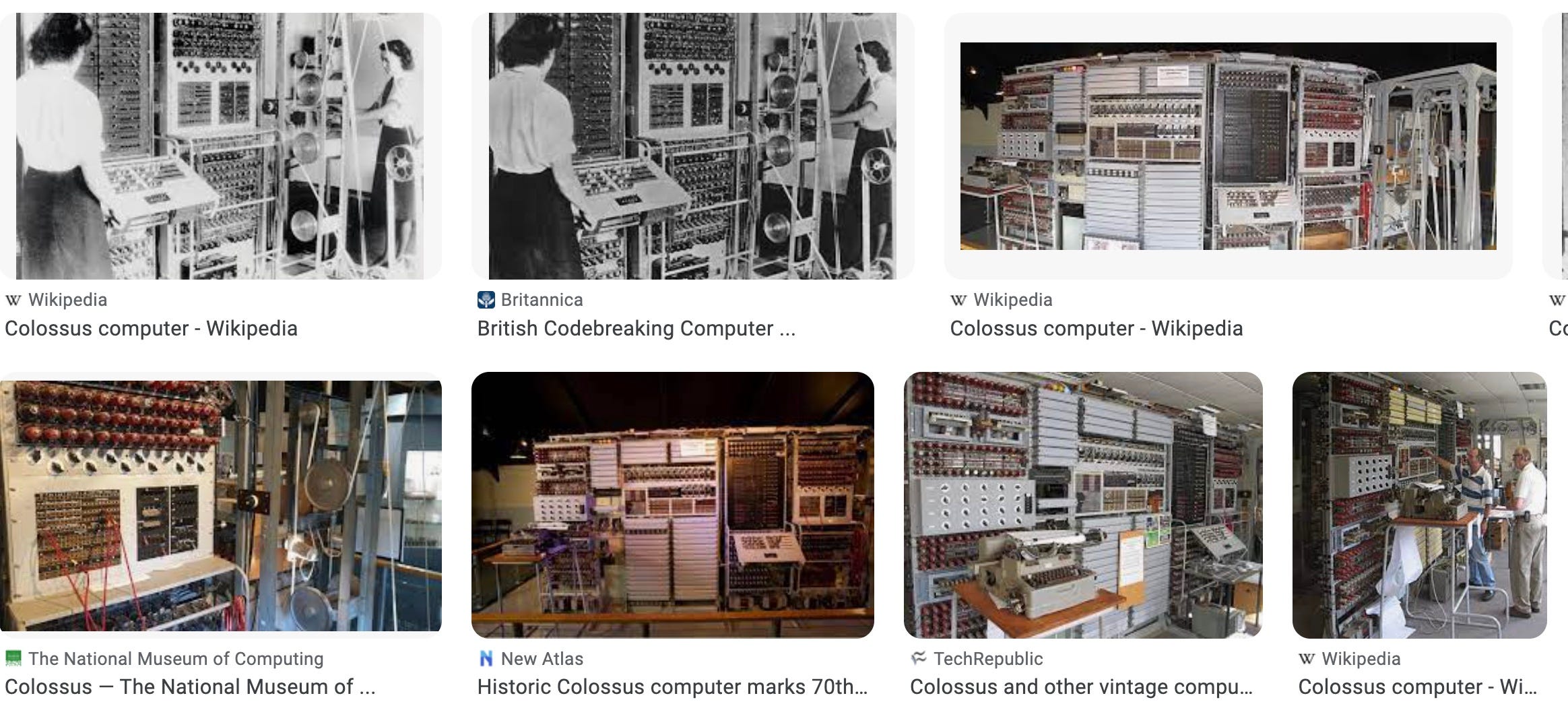
I also like this Colossus !POP figure, hence I mentioned him he’s on my computer:

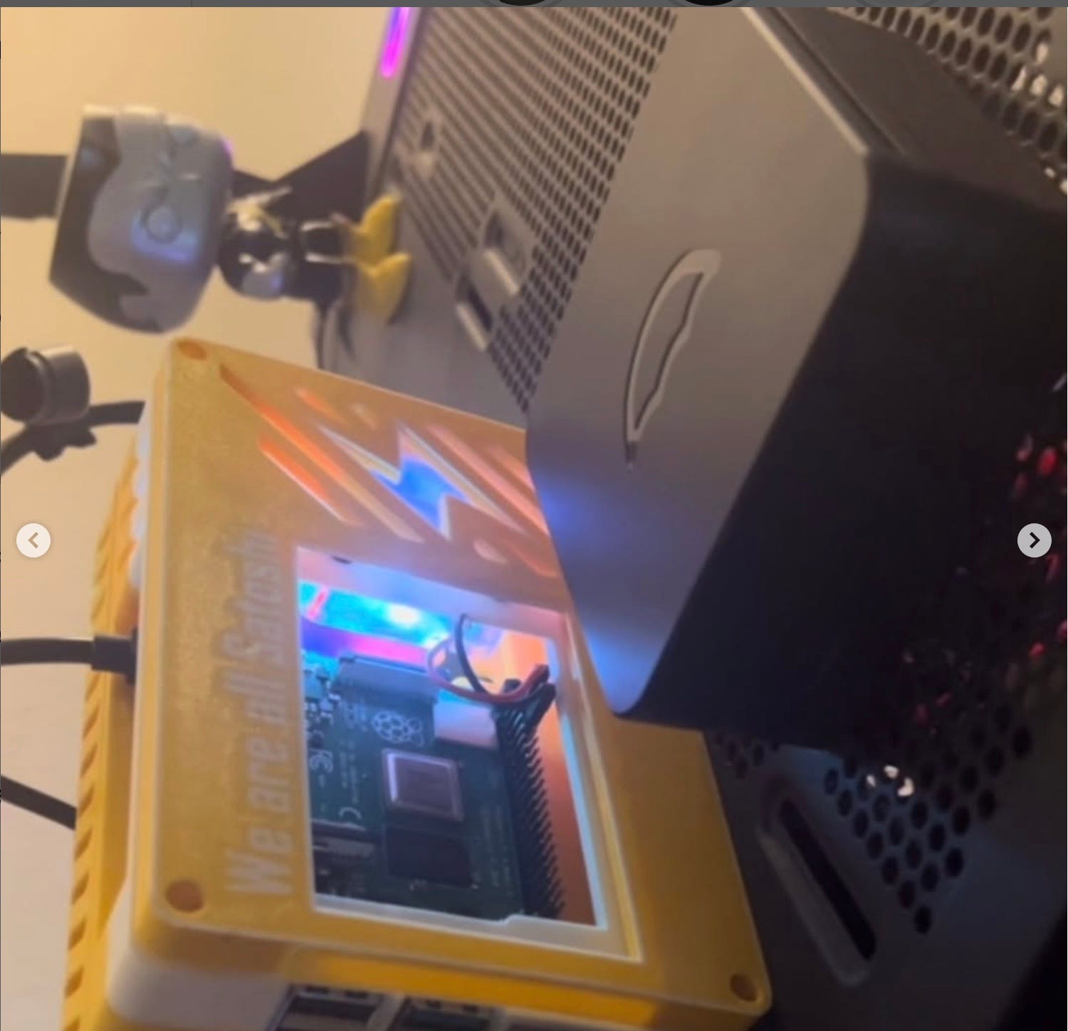
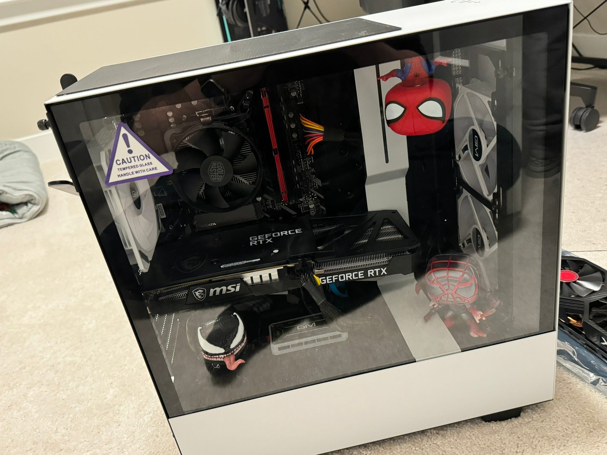
If you want me to build you a cool computer with a cool theme or others you can check out here too, just let me know I’ve been working on this bespoke/side project too.
but I won’t digress further (buying plastic is also kind of cringe),
Another computer was also inspired by a literal dream around the same time (see my later references to the phenomena of simultaneous discovery).
That computer was the ENIAC, rendition of Eckert having the dream:

(credit The History Channel)
“The story associated with the creation of the ENIAC (Electronic Numerical Integrator and Computer) and the Colossus during World War II. Is often associated with J. Presper Eckert, one of the co-creators of ENIAC. As the legend goes, Eckert had a dream during which he saw a soldier pointing at an artillery shell. This dream allegedly inspired him to consider the use of electronic computers for calculating artillery trajectories.”
I will continue to compile many of my notes here including how computers work… and keep proofreading it all, from computer architecture classes and more.
This will be an evolving article as I compile from the inception to the latest in computer science breakthroughs and curate what I find to be the best stuff.
Here’s my summary of how computers work…
If I can explain in the simplest way they sort of brute force calculations in what’s known as the “fetch, decode, execute” cycle. It fetches information you give it, decodes it, then executes all its commands at breakfast speeds. Also, it’s based on the architecture we’ve been iterating on for quite some time, but some basic principles since Alan Turing devised as well as the Von Neumann architecture, here’s some more details,
As a side note this is also one of my favorite scenes from a movie when Alan Turing played by Benedict Cumberbatch, in this dramatization realized they cracked the Enigma machine with the machine Turing designed at Bletchley park called the “bombe,” after toiling away to create his machine (a computer) as others were attempting math with pens and pencils… He realized implementing, he didn’t even really need to know German— he only needed to know how they would type the weather, and decoded all of it that way. A process of deduction and his genius.
The Bombe was an electromechanical device used by British cryptologists during World War II to decrypt messages encrypted by the German Enigma machine, it was a critical tool in breaking the Enigma code and played a significant role in Allied efforts…

"Image courtesy of 'The Imitation Game' (2014), directed by Morten Tyldum.”
Alan Turing had already wrote significant contributions on his programmable computer paper that made the rounds in academia before this accomplishment during the war when he was 27…
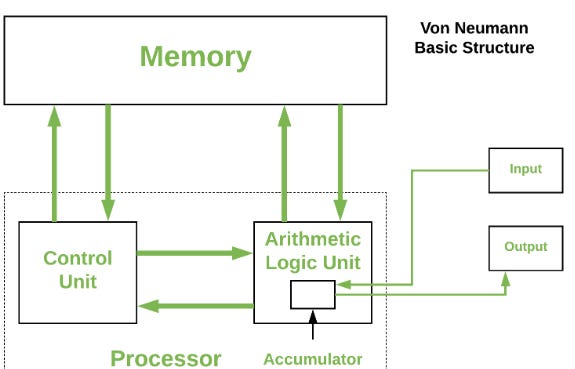
Von Neuman’s architecture that has played a significant role in modern computing architecture as well, an infographic:
Continuing…
Computer Architecture Synopsis and Insights:
Some of this is aggregated notes and questions from a college course with questions/answers, posting all here, enjoy!
Describe the functions that each of these components performs and how they interact with each other at a high-level?
The Central Processing Unit is the "brain" of the computer. I somewhat disagree with that generalization as the storage device of the computer would also encompass the majority of what would be our "memories" and between the smaller and bigger hippocampus' and regions of our brain would be segmented into what could be considered our RAM as far as "short term memories." So a computer would be interacting with those other specific components (if not all handled in some kind of ARM architecture) through the transistors, circuitry, carbon, and other precious minerals that makeup and are used to manufacturer modern computers and devices- as opposed to a brain with our biological brain matter and billions of neurons. However, the text does immediately go into lots of specifics and very good technical explanations that allow us to deduce that the CPU is where a majority of the calculations occur for the computer. As part of its makeup as many PC enthusiasts know the pins attach to the correct socket for that manufacturer and within the body of the CPU these pins are able to communicate and the CPU has that structure to it with the registers in the way it routes and computes huge amounts of calculations that allow it to ensure the computer can run a part of its ever-increasing with Moore's law hundreds of millions of instructions per second (fun fact the human brain clocks in at 10^15 instructions per second, give or take).
The Control Unit is the part that controls the input and output, runs all the necessary computing power to maintain the functioning of the I/O of the "computer" wherever that is as far as in a desktop computer or inside an ARM chip for a mobile device, or some other device.
The Arithmetic Logic unit is the part that does the heavy lifting. Making all those millions and now billions of calculations a second, measuring by MIPS, for instance, an i7-4770k from 2012 would compute 133,740 MIPS and more recently a core i9-990k would be 412,090 MIPS and some commercial desktop processors from now 2020 such as a Ryzen Threadripper with Zen architecture can be 2,356,230 MIPS. I believe the fastest supercomputer currently is 415.53 petaflops, housed in Japan and used in helping with COVID-19 vaccine development, as a lot of AI used such as in NVIDIA GPUs have also helped with gene sequencing etc. apparently. I guess the petaflops and MIPS calculations are similar as far as MIPS is integer calculations and the petaflop number is floating point operation per second, being mutually inclusive, it looks like.
The special and general purpose registers look like the logical route the instructions take, as per that image in the text... https://usercontent1.hubstatic.com/8426680.jpg
The Data Bus goes back and forth the control signals go in (from Control Unit), data values are returned, data values go into the register from the ALU and returns operands back out to the ALU. It is the temporary storage area.
It seems to be, having an agreed upon and developed number of general-purpose registers, not having too many is beneficial. As far as if you have too many the instructions have to become too complicated, whereas up to a certain amount as it tends to sort of encompass a market share- for instance the 64-bit platform on this- more and efficient applications of it can be made. Like with the current state of quantum computing so far as I've read into it's hard to find a general use case for them using it in practical applications and making things for it is too intractable. While something like 64-bit just has more resources and support (as more modern, continuing and successful development on it). I think I'm looking for a different term to describe that there but can't seem to remember...
The general-purpose register or MSR is among this temporary storage area where instructions such as from the RAM come in and are accumulated for example and assigned different functions, while the special purpose register SPR helps hold the program states or correspond to specialized hardware elements...
Give an example using the following Assembly language instruction: ADD R3, R2, R1 (Hint: What task/action does the CU, ALU and Registers perform to execute this instruction?)
ADD R3, R2, R1 adds the second high byte… the first of the low-bytes lower nibble, and R1 the second of the two high-bytes… As a part of this assembly language command these can be very efficient commands as in assembly language the instructions are executed no matter what as they are given and you utilize the places in your register as exactly as you need them and may be further allowed by SRAM and they are available the ALU is the accumulator and the CU is the Control Unite where the commands are held… This command is a usage of Binary Coded digits to accomplish according to the AVR Assembler Tutorial as far as I understood thus far...
What is the difference between main memory and registers? (Hint: Examine their construction and purpose.)
The main memory is a part of a physical component that is RAM usually held separately from the CPU, it is where the CPU can receive instructions to carry out the fetch-decode-execute cycle.
Within the CPU the registers are built within it, it’s its own kind of RAM (but not RAM) inside of the CPU- where data is held or temporarily stored in these registers and the data is being fed into the CPU to be worked on.
I like to think of the fetch-decode-execute cycle as to how modern computers based off the science in the first computers such as the ENIAC and Collusus from the late 30s into 40s that have been ever increasingly using calculations as a way to “brute force” this ever-advancing technology to do what we want. The technology expansion these various time periods in computer history are also pretty interesting as far as the concepts of "multiple discovery" or "simultaneous invention." There is a wiki article with the title of those terms in quotes, that as well as another interesting one describing the "traitorous eight," which were a group of scientists that had left their current employers to work together and produce the worlds first new semiconductors used in modern computing.
... The CPU is receiving this large data and then all the way down to the bits computing these massive amounts of information (fetching) then calculating it (decoding) and then forms this route in the architecture to execute and return these data values that have culminated into modern computing and user-friend GUIs… (I will probably be further reading into the literature to try to get a better understanding of all that is presented, and come to a more intuitive understanding) because let’s be honest it kind of feels like magic!
Mine above
Below
Computer is a machine that does different function through the program instruction in the form of soft ware or hard ware. Instruction input will be processed and result in an out put as soft and hard copy. Hard ware is the physical component of a computer like process, memory devices, monitor, and keyboard ( GeeksforGeeks, 2018). In general computer function as input, process and output.
CPU is called the brain of the computer “ it is the control center of the computer. CPU execute or performs the required computation and then either stored the output or displays on the output device ( GeeksforGeeks, 2018).. CPU has three basic components, which are Control Unit (CU), Automatic Logic Unit (ALU), general and special purpose registers.
Control unit coordinates and controls the data flow in and out of CPU and also controls all the operations of ALU, memory registers and also input/output units. CU works as gatekeeper and organizer to make sure the operation is completed as instructed. Arithmetic logic unit performs mathematical calculations and takes logical decisions for example addition subtraction and multiplication and division. Logical decision involve comparison of row data items to see which one is larger or smaller or equal ( GeeksforGeeks, 2018). Registers is used to store data used for process, this data could be instruction to be processed by ALU. There are special purpose and general purpose registers, General purpose store data or memory location address and special purpose is meant to hold either data or memory address only but cannot be used to store both( Patil, 2019) . The three component work in coordination to fulfill the function of CPU.
The assembly language ADD, R3, R2, R1 is instruction and process happening inside the CPU. For example ADD is performed at the ALU which instruct to add value to register R1 , R2 and R3. The control unit coordinates the execution of the instruction from the ALU to registers.
Registers can be defined as temporary storage locations,. General-purpose register can store a data and it is multipurpose register, which can be used by programmer or user. Special purpose register is for specific purpose for example stack pointer, program counter and instruction register. The advantage of many register can optimize instruction size and speed and the disadvantage is it adds a bit of complexity to compilers (Heggie, 2017). The advantage out weigh the disadvantage having many will increase the processing speed.
The purpose of main memory and registers are to hold data. The difference between the two is as follows. Main memory is hardware device used to store computer programs, instructions and data. It can be internal and external memory to the processor example RAM and Hard drive. Registers are the smallest data holding elements that are built in to the processor. These are the memory locations that are accessible by the processor (GeeksforGeeks, 2020).
The CPU of a modern computer consists of a variety of components. The most major to note is the Control Unit, which is in charge of operating the CPU itself. Along with that are the registers, containing data relevant to the computer, and the Arithmetic and Logic Unit. The latter particularly works out mathematical and boolean operations, as part of the CPU components. All these interact with each other using CPU interconnection communication— The CU can access the registries of data in the general purpose and special purpose registries, and communication occurs through three different control buses: the Data Bus, Control Bus, and the Address Bus. The Data Bus is a bidirectional communication between the MDR and memory. The Address Bus is unidirectional between MAR, I/O ports, and memory. The Control Bus sends control and interrupt signals with the I/O, memory, and the Control Unit.
With the code ADD R3 R2 R1, the Control Unit decodes the program and sends the command to the ALU to add a value from the registry R3, then repeats for R2 and R1. The registries retain this data until it is no longer needed or the machine has lost power.
The difference between Main memory and the registries is the fact that registries are smaller in capacity but provide a faster, more ease of access to the memory it holds. This is a crucial part of design decision making as the developer must consider time against size when deciding how to utilize it. Using a memory hierarchy, it enables prioritizing the needs of the program for its usage with both systems delivering based on those qualifications. The hierarchy starts with registers, cache, and main memory, which are all part of the main board. The further down it goes, the cheaper the cost gets, the less frequent it is accessed, and the capacity becomes larger, along with the amount of load times. On top of that, registries may be visible to the user, or used only by the CPU, for control purposes.
Special purpose registers exist to give dedicated memory usage for specified usage, while general registries are available for all data, values, parameters, etc, to be used as needed. Registers consist of AX, CX, DX, BX, SP, BP, SI, DI. Having a few general registries can limit the option for the computer to access memory without having to go through DRAM or ROM, which has a slower bus transfer speed. However, the use of too many caches can complicate the design process.
In a computer one of its many components and probably the most important would have to be the Central Processing Unit (CPU). It carries out the many instructions of a computer program, whether it being mathematical, logical and input /output (O/I) operations. Within the CPU it also contains various components, one being the Arithmetic Logic Unit. As the name states, it is in charge of mathematical functions such as addition, subtraction, multiplication and division. It also performs logical actions. All the information that is computed through the ALU is then stored in the registers of the CPU. Registers are built into the CPU itself and allow for data to be stored within them. Different types of registers exist on the CPU, and example would be general and special purpose registers. The last component of the CPU is what is in charge on how to use the data, the Control Unit (CU). The CU is what manages the activity of what happens in the CPU. When information comes in, it tells the ALU how to use that information and moves the data between ALU and registers.
Assembly language is a human readable machine language. “ADD R3, R2, R1” is a label and its operands. This information is be distributed, the operands R3, R2, R1 will go to the ALU, then the CU will instruct the ALU on what to do with operands. In this case, the instructions to the ALU will be to add R2 + R1, then move the value to R3. The registers will hold the information and the CU will determine how it is used.
Main memory is a hardware device that is used to store computer programs, instructions and data. The CPU interact with the main memory but at a slower rate than Registers and is only in use when the power is on. Registers are built into the CPU itself, which give the CPU faster access to the information it is currently using.
The need for having both special purpose registers and general purpose registers are to control and distribute information. General purpose registers hold temporary information that the CPU can access and its task can be changed by the programmer. Special purpose registers have a more defined tasks and usually are not accessible by the programmer. Their predefined functions can vary, one such task is to work with the Operating system (OS), storing information that is required for system-wide data functions.
There are several disadvantages to having too many registers. The instructions encoding space is taken up and expands with every new register. This can cause latency and possibly the slowing of CPU performance. Expense is also increased with adding more registers, not only in the production process but there is also an excessive amount of power that is used.
Computers are quite complex and are used to accomplish an abundance of tasks. The Central Processing Unit (CPU) is essentially the brain of a computer and orchestrates the accomplishment of these tasks. The main components of the CPU include the control unit (CU), arithmetic logic unit (ALU), and registers.
The control unit acts as a “director”, controlling the flow of data by converting instructions received from memory into signals which tell the processor to accomplish some task or function, and then monitors the execution of that function (Singh, 2019). The arithmetic logic unit is used to conduct arithmetic (add, subtract, etc.) and logic (and, or, etc.) operations within the CPU. The ALU receives data and instructions from the control unit about what operations must be performed, and outputs the results to memory (Computer Hope, 2020).
Registers are small memory storage units which are directly accessible by the CPU. These are used by the CPU to store data as it undergoes operations. Two particular types of registers are special and general purpose. Special registers are typically used to track the program state and is similar to following a set of instructions (which includes each operation and its memory address). General purpose registers, simply put, are used to store addresses and temporary data such as that used during arithmetic operations (Syed, 2020).
To demonstrate how these components work together, we can use the example provided in the assignment: “ADD R3, R2, R1”. To break this down simply, “ADD” is our function which means we are adding some values. R3, R2, and R1 are our general-purpose registers. So, this syntax is telling the system to add the binary values found in registers R3 and R2 and store the result in R1. Because it is an arithmetic function, the CU will pass it to the ALU. The ALU will add the values and then store the result in the R1 register as instructed (Hickey, 2001).
Although registers and memory are both used to store data, they are quite different from one another. The primary difference between registers and memory is the type of data held. Registers only hold data that is actively being processed by the CPU. However, memory generally holds the instructions and data that the CPU needs in order to execute a process. Additionally, registers are small and hold up to 64 bits of information. But memory is quite larger and is now easy to find in gigabits and higher. Another difference is speed. Because registers are small and easily accessible by the CPU, they are much faster than memory (GeeksforGeeks, 2020).
As previously mentioned, special- and general-purpose registers serve an important role for the CPU. Being easily accessible by the CPU, they can help speed up the processing of instructions and data. However, the number of registers requires a balance. Too few and only a couple of tasks can be processed at a time. However, using too many registers can increase the complexity to a point where efficiency becomes degraded because more space is used just to hold the source and destination instruction addresses (source and destination) (Ripley, 2011).
Discuss the difference between a translator, interpreter, assembler, and a virtual machine:
A virtual machine is in essence a computer that is running often in a different location, or sometimes as an instance of an OS on the same machine too- to accomplish a task, like if the running system is a box, it is a box within a box to specifically accomplish some task.
The assembler takes all the instructions and assembles in a format so the computer can interpret, as a computer is an inanimate object and can’t necessarily understand the english language and how people speak in easy-to-read sentences, it has to be fed to through the architecture of the computer effectively so it can complete the task we’re telling it to run. The assembler is what’s dishing out the machine code
The interpreter and translator are the other steps to this process. It is basically like you’re throwing your instructions into a mesh fabric, and this mesh fabric is splitting what you’re throwing at it so that once it’s fed through it’s split exponentially into more pieces that what’s on that other side of the fabric- what is essentially huge cogs in a wheel spinning at high speeds to perform that task your throwing at it. The interpreter is something that can take what you’re throwing at it and immediately execute, so it’s basically faster. The translator is more of an all encompassing term that makes up these other things you refer to as the compiler, assembler, and interpret as it’s taking your software code and it is a tool that converts it to that the processor can understand.
Describe steps taken by the processor and the responses of the memory controller for each of these operation:
The steps are illustrating the bi-directional and uni-directional computations as they are signals that are transferred among the simple process and memory controllers. The timing diagram is showing the simple process and its relations in a very straightforward way and illustrates how each operation is going between the different buses.
It’s showing the read and write operations, there is the unidirectional 24 address, length, read, write, and enable into memory then the bi-directional routes of a 32-bit system data bus, and Rdy uni-directional. So it’s showing the word sizes of that system in the D figure diagram. The last diagram is showing various directional routes , and I believe the address memory routes as they’re going between the memory cycle and so the timing of the data bus and the read write routes and addresses show a very nice breakdown and lower-level understanding of how this memory is interacting directly with its various buses and how it sends information, visualizing its architecture and the lanes the data is transferring.
Give the Java statement that produced the NASM assembly code and explain:
A //we’re storing the A and moving it to eax
C //doing the same on C
A - A + C // we’re doing an add in assembly of the previous established
A = A + 16 = (A + C + 16) // we’re doing more ADDS with 16 as per the ADD eax, 16 line
A = A - A = (A + C + 16) - (A + C + 16) // performing the SUB of the eax and eax stored values
B + (A + C + 16) - (A + C + 16); // now we’re doing a MOV assembly command on the rest as per the final line
Part 3
section .text
global _start ;must be declared for linker (ld)
_start:
mov eax,3 ; Number bytes to be summed
mov ebx,0 ; ebx will store the sum
mov ecx, x ; ecx will point to the current element to be summed
top:
add ebx, [ecx]
add ecx, 1 ; Move pointer to next element
dec eax ; Decrement counter
jnz top ; If counter not 0, then loop again
done:
add ebx, '0' ; INSTRUCTOR’S QUESTION: Why are we doing this?
mov [sum], ebx ; Done, store result in "sum"
display:
mov edx, 1 ; Message length
mov ecx, sum ; Message to write
mov ebx, 1 ; File descriptor (stdout)
mov eax, 4 ; System call number (sys_write)
int 0x80 ; Call Linux kernel
mov eax, 1 ; System call number (sys_exit)
int 0x80 ; Call Linux kernel
section .data
global x
x: db 6
db 7
db 9 ; editing the array in assembly so as to output the correct ASCII code for F
sum:
db 0
Discuss the difference in machine code, assembly code, and high-level languages.
Describe the steps in compiling a C-program.
High level languages often interchangeable between scripting and programming are very arguably the easiest and most definitive way to interface with various computing platforms.
Whether it’s Objective-C for Mac and Swift, C++, C#, Python, Ruby, Javascript, React, many of the post popular programming languages are all high level programming. Throughout the years and depending on the type of application you’re trying to create will use a variety of these high level languages within an integrated development environment and often in an agile development workflow with many other engineers that have forks and pull and push the various code blocks- creating an intricate code library or repository depending on what kind of applications are using, notating al their code so they can work together too accomplish some task- like huge creative problem solving endeavor.
Machine Code is the very base level code of the computer that encompasses all the 0s and 1s, all the bits of information that the machine itself computes, massive amounts of information at a time that is impossible for a human to fathom and write a modern application in what would be called a timely manner
Assembly Code on the other hand people can interface with at a base level to change and interface instructions in a more reasonable way directly to a computer, as the computer will execute any assembly code just as it is written, and whoever is inputting it in can enter assembly in such a way so that computer executes exactly what they want as long as it’s written properly.
Compiling a C program, just as any program if you’re using an integrated development environment or compiler it requires different stages to be executed correctly to be compiled successfully, these stages include the steps processing, compilation, assembly, and linking.
The initial syntax and semantics are run through the processing stage, it’s a pre-step to to compilation when the instructions are actually compiled and translated into machine code to be executed, then at the assembly change the assembler is used to correctly translated these instructions into object code. As per most object-oriented design they are made of instructions in correct syntax and a logical formula split between instantiating variables, calling a library, methods, and functions (whatever encompasses your C program) that all fit together nicely and then the assembly portion of compiling a C program outputs the instructions to ge run by it’s target processor- linking uses the object code that’s created and fits it all together so that the functions, the libraries and all these are called correctly and the end result becomes the program you can execute/run/
What is the difference between an address bus, data bus, and control bus? What roles do they play and how do they work together to perform a read or write operation? Provide an example of them working together.
When a CPU is said to be a 64-bit processor, what does that mean? In general, what is the word size and how many addresses can it theoretically support? Explain.
How many byte-addressable addresses can a 32-bit processor support that has 20 address lines on the address bus between it and main memory? Explain.
The term bus and the three different designations of the control bus, address bus, and data bus can be rather confusing at first glance. Overall, the term bus describes an exchange of many different data signals, it’s kind of a term to designate that a lot of things are going on- lots of information is being sent back and forth. These three things make up the system bus, the way the CPU, Memory, and i/o devices of the hardware and communicating with each other that ensures the proper functioning of the computer. The control bos is the only of the three that is bi-directionatl as it is communicating with the CPU and the CPU is making all these calculations nad deciding what all is being sent back and forth. The address bus and control bus on the other hand are unidirectional and the address bus is telling where these signals are supposed to go from the processor towards the memory. The data bus is like a barometer that sets what can be the total amount of data delivered at a time. A CPU with a 64-bit processor is used in most modern machines and the data bus is also determinate by this platform as it can compute 64-bits of data at a time. A 32-bit machine is more common in mobile and less powerful devices like with ARM architecture or in many portable and affordable machines- like many laptops limited to 4GB of RAM. the amount of addresses it can theoretically support on a 64-bit process is 2^64 bytes of addressable memory- that’s quite a large number and as we often get into the nitty-gritty of things like astronomy or the base level communications of modern machines as they are continuously excelling in their computational power we start to talk about numbers on the quadrillion, quintillion, even surpassing higher numbers we almost never use in vernacular language like quindecillion- These numbers are often hard to imagine as 10^48 let alone to the 64th power is obviously a number with lots of 0s….
A 32-bit process addresses 2^32 that has 20 address lines as the 20-bit address bus allows for more, being exactly 4,294,967,296 total, as it is more bits used becoming a more efficient use of memory since it has a larger address bus that can compute more information- in the traditional byte-addressable method where a single byte is eight bits of course- and the words “word size” is a terminology for the processor’s exact amount of storage, or rather the smallest size of addressable storage it’s able to compute and send signals back and forth from all the buses as it relates to the dynamic von neumann architecture the machine is able to utilize to effectively execute and perform a task- a 64-bit machine and 32-bit machine have it’s different caveats but a 64-bit machine is generally more capable- as we discussed previously in the class, these are platforms with agreed upon requisites that we've developed massive support on to very suitably execute applications as practically as possibly, based on basically over the some 40-50 years of human engineering where we've written increasingly and increasingly complex applications that run at these insanely high machine computing speeds utilizing these bit structures.
An example of the address bus, the control bus, and the data bus working together is the data bus is travelling through between the CPU, memory, and peripherals i.e. a keyboard, mouse, maybe even a headset, or USB hub and it’s also determining the speed of data travelling - the Address bus meanwhile is determining the max amount of addressable information as designated by the system’s specifications and where in the main memory these operations are assigned or stored and the control bus is carrying the information between the CPU and other components of the computer such as where it is reading from the RAM - and all this is like an information highway of data signals all simultaneously and harmoniously being sent back and forth so as to ensure the proper functioning of the machine so that whatever applications and devices the person using all run properly.
What were the most compelling topics you’d like to summarize?
I think the most compelling things I learned are the history of the first computers and machines. I like this topic as it builds history onto the fabric of what has become so many hundreds and hundreds of devices and platforms in the modern world. It’s also fun to think of the phenomenon of simultaneous discovery, as certain milestones of technology are reached and our capability increases over time to make more advanced systems it’s interesting that many early computers like the ENIAC, the Z3 Computer, things like the Collusus computer that were “turing-complete” machines were essentially developed all around the same time in the early 40s. I’ve taken a couple classes on the introductory to programming and others that introduce the basis of the machines, but I feel that it’s important sometimes to try and retain as much information as possible as it relates to the base-level concepts that formulate how exactly a machine is engineered- so as that if you have I guess I can say full stack understanding of the way whatever machine you’re working - whether it be something like a car, a computer, or even a rocket or a plane then when you’re engineering or developing on these platforms looking to make them run more efficient or help make strides in the field- if you have this base-level understanding then you operate so much more efficiently and can so easily iterate and contribute to a team in an effective way. Basically understanding the intricacies of something like the von neumann architecture, everything down to the way addresses are stored in memory, all the way up to the higher-level operations- whatever you’re working on you understand exactly what’s going on and can quickly and confidently begin solving a problem.
Is anything still unclear that could be clarified?
Reading peers’ work and reading other people having back and forths is very valuable to me, because it was nice to see how we are all always learning and understanding the concepts together. Often when explained or asked a question I can listen in or rather read in to see it from a different perspective, that may aid in my retention of information going forward. I wouldn’t say anything is still unclear, overall I feel like it will take a lifelong dedication to really try and begin to fathom all the massive instructions going in a computer- and whereas you only may need to know and understand most importantly the applications or workflow of whatever you’re doing, understanding and become a subject matter expert will take constant refreshers.
What approaches could have yielded additional valuable information?
I’m not too sure what approaches can be much better with what we’re currently working with, I think the virtual chats, discussion boards, intellipath, reading all the text and assignments are a great way to learn in a distance learning format - I enjoy having taken brick and mortar classes being able to learn at my own pace - I think maybe as distance learning may become even more prevalent in the modern educational landscape, I’m sure people will begin learning in new VR, AR, and dynamic formats. Perhaps some kind of adaptable learning environment that is incredibly engaging in a way suitable to each student- so that they learn, actively engage often, and retain the optimal level of information. I personally like to see real-world applications as often as possible, I like Linus Tech Tip videos, but lots of production goes into those- and even then after the video is over you’re still left with a few questions on how everything is working together. For example I do like seeing an actually processor plugging in, seeing specifications, seeing the thing turn on- I guess I would like an approach where we see for instance engineers actually in a quick maybe 1-2 hour explanation of what their day-to-day is as far as exactly what programming language they’re using, what IDEs, maybe popular tasks people are working on right now, and how that translates to the exact workstation specifications they’re using- maybe everything from computer science majors working in the entertainment field, to those even maybe creating radar systems for NASA or something cool like that… and maybe even something in between that can be both inspiring and incredibly informative.
What is the difference between programmed I/O and interrupt-driven I/O? Give examples? Which is better and why?
Programmed I/O is like a loop in programing where the data that is benign transferred between a device and CPU both require instructions and in this mode it’s continuously on so the CPU is always waiting for instructions, often a easier go-to way or means of instructions for the computer program as again the CPU is always ready- A interrupt-driven I/O is similar to a flag-controlled loop in programming where instead of just always ready to go back and forth and just waiting for that, the interrupt-driven I/O designates the time to interrupt so that CPU cycles are wasted and the CPU can work directly on the command issued.
Define the history of assembly and current programming languages.
The history of programming languages can often be tracked generationally. As those who were engineers and computer scientists coming of age in the late 70s and into 80s, working on machines as Steve Jobs was making Macs- COBOL, C++, MATLAB, and then Objective C are languages you’ll hear thrown a lot. In modern days as students usually start with pseudo code and then Java or Python these are go to of current programming languages. From here it often depends on what you’re designing for as scripting languages like Javascript, PHP, etc. are popular for web developers and engineers, and then on to those programming in JAVA, C#, or C, or even a combination of many of these also using workflows that are popular with things like Ruby or a combination of many. It’s often interesting to think for instance the engineers who invented the Python language are still very much alive, and individuals in different roles can be subject matter experts in one or several languages maybe a novice in other languages. Also even in recent developments another currency programming language is something like Solidity that is primarily used in blockchain, but shares similarities in syntax to other simple and easy-to-use syntax languages. To define the history of Assembly I guess: it can be tracked back again to the 1940s as mathematicians and physicists who created their theoretical works on how to provide instructions in thes fetch-decode-execute cycles on turing-complete machines. As practically applied in the popularized architectures., assembly language cemented itself in the first generation of pioneering programmers and then i nto the 50, 60s, and then once we break the 70s and 80s Assembly language eventually was improved upon to take our human limitations of computing information off the table allowing us to be more productive and effectively create a complex computer. As opposed to COBOL another what I find to be name-drop language is FORTRAN, as these were sort of the forerunning and pioneering languages on this front that helped form and inform later languages.
Describe the steps in detail that the operating system performs to handle interrupts, including ISRs, the stack, and hardware?
Answer the questions embedded in the sample code above.
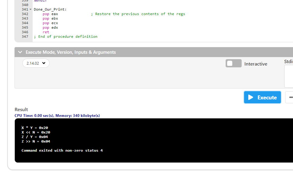
Instructor Question 1: Why is (W * Y) equal to (W << N) ?
Using the assembly language code what we’re doing is shifting numbers in their proper context so that we’re accomplishing the multiplication of Y which in assembly will basically be using that shift value to change that N and multiplying it by the proper value to achieve the Y value from N as per line 25
Instructor Question 2: Why is (Z / Y) equal to (N >> Z) ?
For Z right Shift N, the reason why Z divided by Y is equal to it is because Y is 8 and Z is 16, so 8/16 is 2 and therefore N shifted twice right to Z is also the same. As per their 8 bit values at the binary value and again it shows the same thing, the same binary values.
Hex is displayed on the line calculating the message for the W * Y and it’s allowing a larger string
Instructor Question 3: Why do we do this; i.e. adding ‘0’ to the number?
We are adding 0 to the number in the program, so basically so are converting decimal to ASCII as per the text
Instructor Question 4: What are we doing here? We’re creating a display of a new message in assembly
Modify the code such that if Z = 0x20, then what does N need to equal so that (X * Y) = (X << N) and (Z / Y) = (N >> Z).
Line 22: Z dd 0x00000010
Line 23: Z dd 0x00000020 ; Edited Z to be Z = 0x20
N needs to equal 3 so that the message still holds true: (X * Y) = (X << N) and (Z / Y) = (N >> Z)
I then changed the W values to reflect the new message to X instead, it required me editing lines 202, 206, 192, 188, 34, and 36 replaces the W with X as the new above
Capture screenshots of your source code compiling and executing:
Screenshot of the initial compiling:
My modified compiling: